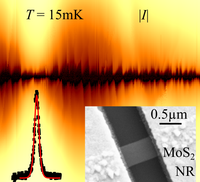
Molybdenum disulfide MoS2 is often discussed as a groundbreaking material for electronics applications. As bulk crystal or as 2D layer material similar to graphene, it is an excellent semiconductor with strong spin-orbit interaction. At strong doping it even becomes intrinsically superconducting, with possibly interesting topological properties.
So how about using MoS2 for quantum electronics, single electron devices, or (charge, spin, or valley) qubits? There's already enough science fiction literature out there mentioning "molycircuits"... Well, a small problem stands in the way. It turns out that the electronic band structure of the material makes reaching quantum confinement, i.e., discrete, addressable electronic quantum states, quite hard. The chip structures need to be built at very small scale, difficult to reach with MoS2 flakes on a chip surface, and so far no research group has managed to do this in a controlled way.
That's exactly why we are interested in MoS2 nanotubes. They can be grown clean and straight, with diameters down to 20nm - which automatically confines charge carriers in one more direction compared to a two-dimensional MoS2 flake. What remains is to restrict motion of the charge carriers along the nanotube axis and to make good metallic contacts. However, it turns out that making good contacts to MoS2 is hard - either your metals form a Schottky barrier, or they react with the MoS2 and destroy its crystal structure.
In our work, we show that this problem has now been solved. Using a thin layer of the semimetal bismuth, we obtain contacts which remain transparent even at cryogenic (millikelvin) temperatures and leave the structure of MoS2 below and next to them intact. This makes transport spectroscopy measurements on a MoS2 quantum dot forming within the nanotube possible. We indeed observe quantum dot behaviour; the temperature dependence of the Coulomb oscillations of conductance indicates that we reach electronic tunneling through single, discrete quantum states below a temperature of T=100mK.
With this, we have made a big step towards controllable charge, spin, or even valley quantum states in MoS2. Next we need to miniaturize our devices even further, and increase our measurement resolution to be able to analyze the electronic level spectrum in magnetic fields.
"Non-destructive low-temperature contacts to MoS2 nanoribbon and nanotube quantum dots"
R. T. K. Schock, J. Neuwald, W. Möckel, M. Kronseder, L. Pirker, M. Remskar, and A. K. Hüttel
accepted for publication by Advanced Materials (doi:10.1002/adma.202209333); arXiv:2209.15515
(PDF,
supplementary
information)

No comments:
Post a Comment