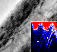
We are happy to be able to announce that our manuscript "Coulomb Blockade Spectroscopy of a MoS2 Nanotube" has been accepted for publication by pssRRL Rapid Research Letters.
Everybody is talking about novel semiconductor materials, and in particular the transition metal dichalcogenides (TMDCs), "layer materials" similar to graphene. With a chemical composition of TX2, where the transition metal T is, e.g., tungsten W or molybdenum Mo, and the chalcogenide X is, e.g., sulphur S or selenium Se, a wide range of interesting properties is expected.
What's by far not so well known is that many of these materials also form nanotubes, similar to carbon nanotubes in structure but with distinct properties inherited from the planar system. Here, we present first low temperature transport measurements on a quantum dot in a MoS2 nanotube. The metallic contacts to the nanotube still require a lot of improvements, but the nanotube between them acts as clean potential well for electrons.
Also, our measurements show possible traces of quantum confined behaviour. This is something that has not been achieved yet in planar, lithographically designed devices - since these have by their very geometric nature larger length scales. It means that via transport spectroscopy we can learn about the material properties and its suitability for quantum electronics devices.
A lot of complex physical phenomena have been predicted for MoS2, including spin filtering and intrinsic, possibly topologic superconductivity - a topic of high interest for the quantum computing community, where larger semiconductor nanowires are used at the moment. So this is the start of an exciting project!
"Coulomb Blockade Spectroscopy of a MoS2 Nanotube"
S. Reinhardt, L. Pirker, C. Bäuml, M. Remskar, and A. K. Hüttel
Physica
Status Solidi RRL, doi:10.1002/pssr.201900251 (2019); arXiv:1904.05972
(PDF)
Monday, August 12, 2019
Tuesday, July 2, 2019
Where's the best sciences research in Germany? Here in Regensburg!
The Nature Index 2019 Annual Tables have been published, and there is a valuable new addition: the tables now include a "normalized ranking", where the quality of a university's research output, and not its quantity counts. If we look at the world-wide natural sciences ranking, University of Regensburg is at spot 44, best of all universities in Germany, and in a similar ranking range as, e.g., University of Oxford, University of Tokyo, or University of California San Francisco! Cheers and congratulations!
Labels:
physics,
regensburg,
research-group,
work
Thursday, May 2, 2019
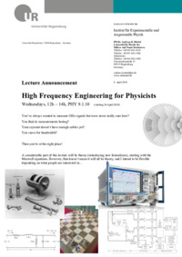
Lecture announcement: High Frequency Engineering for Physicists
Term has already started, so this announcement is technically a bit late, however... This summer term I'm offering a lecture "High Frequency Engineering for Physicists". If you plan to work with signals in the frequency range 10MHz - 50GHz, this might be interesting for you...
See you next wednesday!
When and where? Wednesdays, 12h - 14h, seminar room PHY 9.1.10. The next lecture is on 8 May 2019
- Concepts and formalisms for the frequency range 10MHz - 50GHz
- Handling equipment for this frequency range, designing devices and measurements
- Using this frequency range in a (millikelvin) cryostat
See you next wednesday!
Labels:
physics,
research-group,
work
Tuesday, April 30, 2019
Press release (in German) on our recent PRL
Regensburg University has published a press release (in German) on our recent Physical Review Letters "Editor's Suggestion" publication, "Shaping Electron Wave Functions in a Carbon Nanotube with a Parallel Magnetic Field". Read it on the university web page!
(A summary in English can be found in a previous blog post.)
(A summary in English can be found in a previous blog post.)
Labels:
nanotubes,
physics,
research-group,
work
Wednesday, February 27, 2019
PRL published: Shaping electron wave functions in a carbon nanotube with a parallel magnetic field
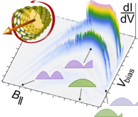
We're happy to announce that our manuscript "Shaping electron wave functions in a carbon nanotube with a parallel magnetic field" has been published as Editor's Suggestion in Physical Review Letters.
When a physicist thinks of an electron confined to a one-dimensional object such as a carbon nanotube, the first idea that comes to mind is the „particle in a box“ from elementary quantum mechanics. A particle can behave as a wave, and in this model it is essentially a standing wave, reflected at two infinitely high, perfect barrier walls. The mathematical solutions for the wave function describing it are the well-known half-wavelength resonator solutions, with a fundamental mode where exactly half a wavelength fits between the walls, a node of the wave function at each wall and an antinode in the center.
In this publication, we show how wrong this first idea can be, and what impact that has. In a carbon nanotube as quasi one-dimensional system, an electron is not in free space, but confined to the lattice of carbon atoms which forms the nanotube walls. This hexagonal lattice, the same that also forms in planar form graphene, is called bipartite, since every elementary cell of the lattice contains two carbon atoms; one can imagine the nanotube wall as being built out of two sub-lattices, with one atom per cell each, that are shifted relative to each other. Surprisingly, the hexagonal bipartite lattice does not generally support the half-wavelength solutions mentioned above, where the electronic wave function becomes zero at the edges. In each sublattice, we can only force the wave function to zero at one end of the nanotube "box"; its value at the other end remains finite. This means that the wave function shape for each of the two sublattices is more similar to that of a quarter wavelength resonator, where one end displays a node, the other an antinode. The two sublattice wave functions are mirrored in shape to each other, with node and antinode swapping position.
When we now apply a magnetic field along the carbon nanotube, a magnetic flux enters the nanotube, and the boundary conditions for the electron wave function change via the Aharonov-Bohm effect. Astonishingly, its shape along the carbon nanotube can thereby be tuned between half-wavelength and quarter-wavelength behaviour. This means that the probability of the trapped electron to be near the contacts changes, and with it the tunnel current, leading to a very distinct behaviour of the electronic conductance. It turns out that our measurement and the corresponding calculations are agreeing very well. Thus, our work shows the impact of a non-trivial host crystal on the electronic behaviour, important for many novel types of material.
"Shaping electron wave functions in a carbon nanotube with a parallel magnetic field"
M. Marganska, D. R. Schmid, A. Dirnaichner, P. L. Stiller, Ch. Strunk, M. Grifoni, and A. K. Hüttel
Physical Review Letters 122, 086802 (2019), Editor's Suggestion; arXiv:1712.08545 (PDF, supplementary information)
Labels:
nanotubes,
physics,
research-group,
work
Subscribe to:
Comments (Atom)


